Board Editor
To launch the schematic editor click on “Board” in the project manager.
The board editor keeps an internal copy of the netlist. To update the netlist, click “Save” in the schematic editor for writing the netlist to disk, then click on ’reload netlist’ or re-open the board editor or use the action “Save and reload netlist” in the the schematic editor.
Planes
For adding planes, first draw a polygon of the desired shape in a copper layer. Then use the “Add plane” tool to assign it a plane. Planes with lower fill order will get filled first. To override the connection style (solid or thermal relief), create a Thermal rule.
Vias
To place a via while routing, press v. The “Layer pairs” rule defines which layer the router switches to. To change the size of vias, define a matching via rule or via definitions.
You can also place vias not connected to any track with the “Place via” tool.
See Vias for how to use blind or buried vias.
Importing logos
The preferred way to import logos and other artwork into the board editor by means of the DXF import tool. Since Horizon EDA doesn’t support bezier curves, convert these to lines first. Inkscape’s “Modify Path/Flatten Beziers” extension works great for this. If you require filled polygons, use the “Line loop to polygon tool” to convert line loops to polygons. Use the “Scale” tool to adjust the imported logo to the size you need.
Board outline
Define the board outline by drawing polygons on the Outline layer. The board must be representable by a single polygon with zero or more holes, that means:
There must one polygon that encloses all others
These other polygons are holes
Hole polygons must not intersect or touch each other
The “Outline” rule checks that these requirements are met. Do not use arcs or lines on the outline layer. Put any other outline-related information such as indications for v-scores on the “Outline Notes” layer. The Gerber export merges the “Outline” and “Outline Notes” laters.
Reconnecting tracks without a net
For a track to be assigned a net, is has to be connected to a pad or a via either directly or indirectly. If that’s not the case, tracks are assigned to no net and turn orange. Use the “draw track” tool to reconnect the track to a net.
Diffpairs
To create a diffpair see Schematic Diffpairs . Before routing a diffpair, create a diffpair rule specifying track width and gap. To route a diffpair, use the “Route diff. pair” tool.
Nets window
You can open the nets window from the “View & Selection” menu in the bottom bar or by searching for it in the spacebar menu.
Hide Airwires
Uncheck the checkbox in the airwires column to hide the airwires of a net. You can also select more than one net and use the context menu to turn off or on airwires for multiple nets at once.
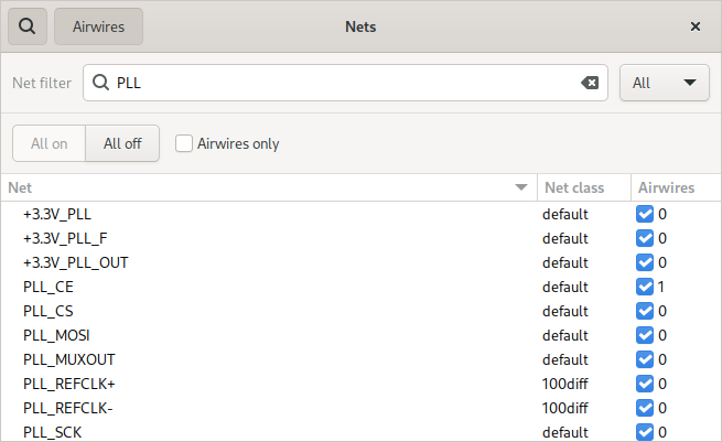
Recolor nets
Right click on one more selected nets to open the context and assign a specific color to nets.
Panelisation
For making best use of the available board space, Horizon EDA supports panelisation. Rather than copy/pasting a board into another one, which complicates last-minute changes, a board can reference other boards.
Panelising an existing board in Horizon EDA is a simple multi-step process:
Create a new empty project and open the board.
Use the “Manage included boards” tool to load the board(s) to be placed on the panel.
Place the included boards using the “Place board panel” tool.
The boards can then be arranged as one object each without the possibility of unintentionally modifying it. To update the included boards, either use the reload button in the “Manage included boards” tool or reopen the project.
For making it easier to draw the panel outline, the outline of included boards can be extracted using the “Smash panel outline” tool.
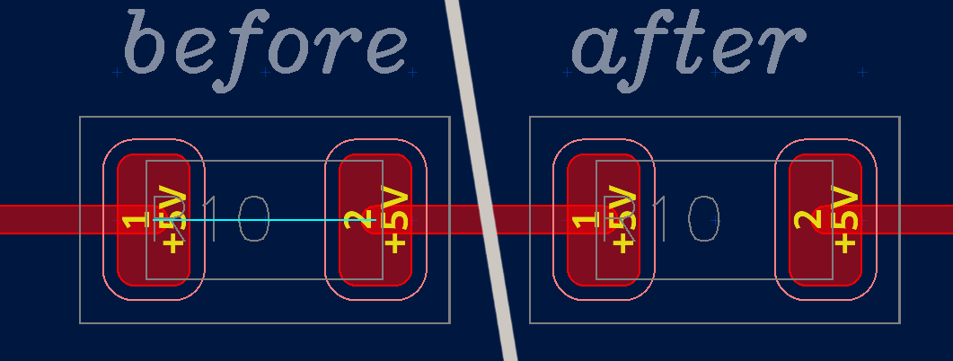
Shorted pads
When using zero-ohm resistors or other components for connectivity, there’s still an airwire across the component since Horizon EDA isn’t aware that the part is a short circuit.
Create a “Shorted pads” rule to specify that the pads of a part are electrically connected.
Net ties
Once a net tie has been defined on the Schematic, it can be added to the board using the “Draw net tie tool”. A net tie on the board behaves similar to a track of the primary net and are treated as such by track width, copper clearance and other rules. Since net ties go from junction to junction, they can be joined with other tracks.
The “Net ties” rule checks that all net ties that are defined on the schematic are drawn on the board and connect to the correct nets. The copper clearance checks ignore the clearance violation caused by the net tie, but still flag clearance violations caused by other objects of the net.
Offset pad connection
For complex-shaped pads, one might want to connect a track to a specific position in the pad rather than to its origin. Use the “Move track connection” tool to move the end of a track that’s connected to a pad.
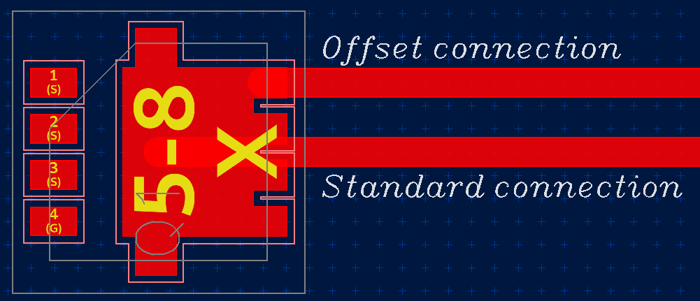
Keep in mind that tools based on the KiCad router such as “Route track” or “Drag track” aren’t aware of this and will break the pad-track connection.
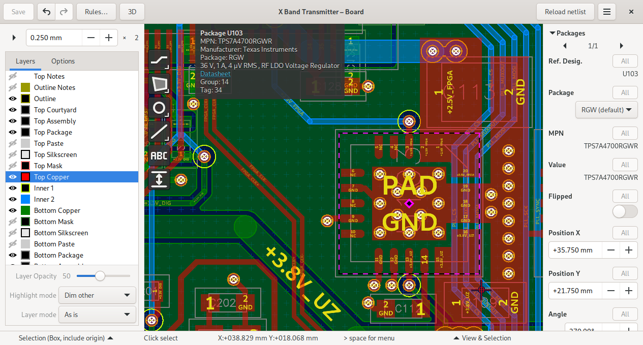
Screenshot